Pioneering the Future of Diamonds

The global leader in high-pressure, high-temperature technology, crafting large human-made diamond crystals and innovative high-pressure equipment. Ethical, sustainable, and uniquely designed for you.

Contact Us Now

Sustainability

Ethicality

Revolutionary

 The global leader

The global leader

EcoDiamond is the global leader in the technology of obtaining large human-made diamond crystals at high pressures and temperatures, and in the production of unique high-pressure equipment. By owning the technology of creating a diamond and the technology of manufacturing the whole set of necessary equipment – including the complete package of constructional and technological documentation and logistics of production – our company provides the fastest and most beautiful diamond creation for any customers’ request.

Research and development

Research and development

No other company can make custom diamonds as beautiful as ours, let alone deliver them as quickly as we do. Additionally, EcoDiamond conducts research and development towards increase in the size of the obtained diamond crystals possessing the highest structural quality and preset properties. The synergies between two key components – technology and equipment – lies on the basis of continuous effective development of EcoDiamond.

A diamond is wide bandgap semiconductor, which allows to achieve new devices with greater power density and energy efficiency. Due it highest thermal conductivity and high carrier mobility it occupies a special place among the other high demanded wide bandgap semiconductors, such as silicon carbide (SiC), gallium nitride (GaN), other nitrides from the group V in periodic table and their triple compounds. A diamond also has a unique role between optical, acoustic materials, radiation detectors, electronic emitters, materials for quantum applications, and other types of high-tech materials associated with a combination of exceptional and extreme physical properties that can only be found in diamonds.

Such a unique combination of extreme properties is a consequence of the nature and crystalline structure of the diamond, which herewith make diamond one of the most difficult technological materials. That is why, despite the enormous high-tech potential that diamonds naturally have, the diamond enters these niches so slowly and with such difficulty. For example: the first step of proving diamond’s potential to influential electronics corporations is already difficult. To impress investors, one must prove the necessity of obtaining high crystalline quality single-crystal diamonds up to two inches in size as a first step. Without this, it is nearly impossible to get the necessary level of financial backing in order to develop the scientific field. This diamond substrate size will allow to use technological converters in the electronics industry, which will open fundamentally new opportunities for the development of diamond electronic structures. Diamonds need to be grown in near-equilibrium conditions – that is, at high pressures & temperatures that create the thermodynamic stability that mimics nature. By using a multi-stage approach, EcoDiamond solves the technological task of cultivation of such diamonds, creating economically viable technology.

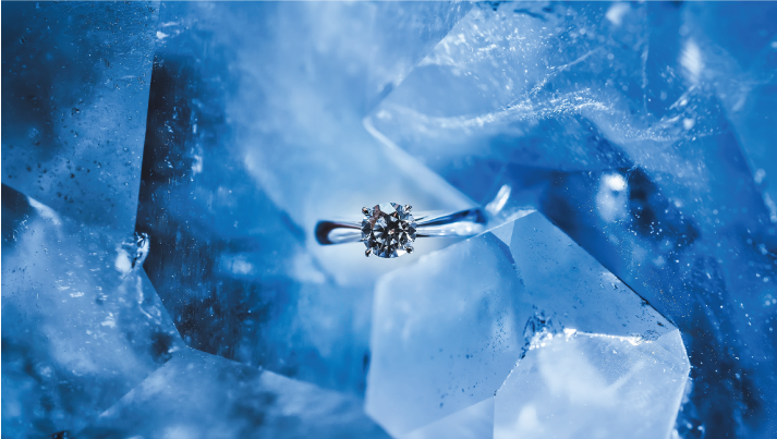
EcoDiamond offers products from grown diamonds under the new brand EcoDiamond, symbolizing the birth of diamonds in conditions similar to natural deep in the hidden caves of the earth – but, at the same time, our diamonds never mistreat the ecology of our planet, nor do they destroy people’s lives, on the way to the consumer.

One of EcoDiamond's priorities is to promote in high-tech markets, as for now the following areas are featured:

EcoDiamond® for high-tech market

Substrates and elements

EcoDiamond substrates and elements are the ultimate choice for developing high-power and high-frequency electronics (Schottky diodes, p-i-n diodes, lateral MOSFET devices), radiation detectors, field and thermionic emitters for power converters, Raman lasers, nanostructures for quantum sensors, and quantum communication.

Single crystal EcoDiamond

Single crystal EcoDiamond substrates for homoepitaxial CVD diamond growth. EcoDiamond substrates can be fully customized for our clients. This includes their impurity content, concentration, and crystallographic orientation for specific application to the CVD diamond. Nitrogen concentration in the electrically non-conductive substrates can be modified in the range from less than 0.1 ppm up to 300 ppm. Boron concentration in the semiconducting substrates can be modified from 1 ppm to 1000 ppm.

Highest structural quality

Due to the highest structural quality, EcoDiamond is the best material to manufacture elements of X-ray optics (prisms, lenses, monochromators, and splitters) for the third and fourth X-ray sources generators in synchrotron factories.

Ultrahigh pressure

EcoDiamond anvils can be used in materials research under ultrahigh pressure.

Special precision tools

EcoDiamond can be used in special precision tools like microsurgical scalpels, microtomes, precision cutters, etc. that would revolutionize the dentistry, surgery, and even the 3D-printing industries (nozzles).

Let's Talk

Got Something on your mind?

Contact Us
Take A Look At Our Other Products
background

Sign up for our newsletter

Be the First to Know – Get Exclusive Updates!